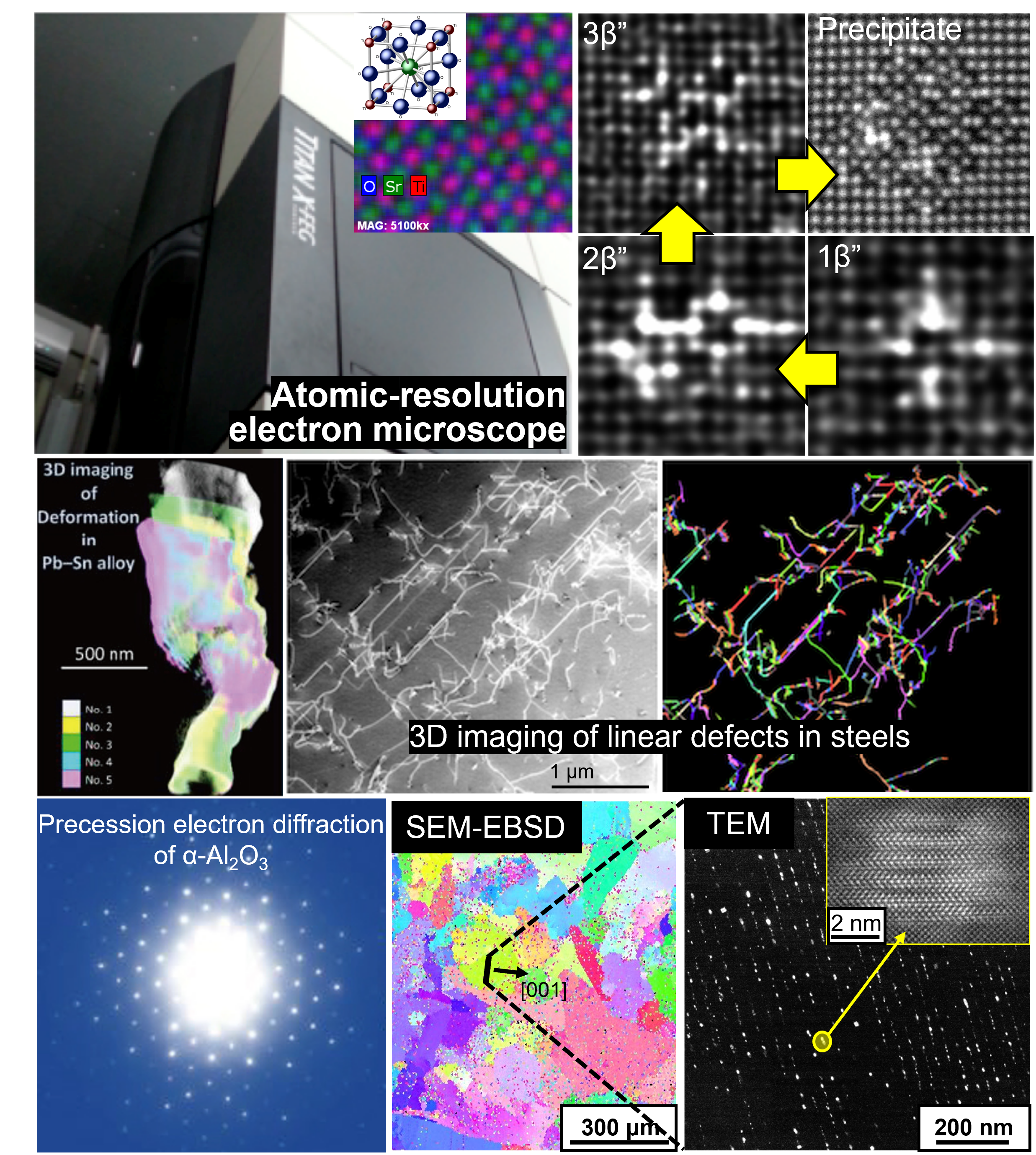
3D Imaging of Crystalline Materials by Electron Tomography
Electron tomography, a 3D imaging method using TEM/STEM, is known as a powerful approach for overcoming the problem of two-dimensional projection and overlap in conventional TEM/STEM images. Our laboratory visualizes dislocations, interfaces, precipitates, and other defects in crystalline materials, including ferromagnetic materials such as iron, in three dimensions to clarify the mechanisms of deformation and microstructure formation.
For more details on our 3D characterization topics, please see here.
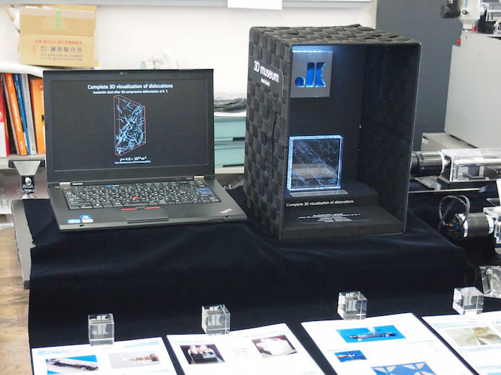
A 3D image of dislocations, line-shaped lattice defects, in steel visualized by electron tomography and printed in glass using a 3D printer.
Produced with the cooperation of Dr. Masatoshi Mitsuhara, Kyushu University, and Mel-Build Co.
Example of three-dimensional visualization of dislocations in steel
Related work: Ultramicroscopy (2017), etc.
3D Imaging and In-situ Observation in Electron Microscopes
We directly observe changes in material microstructures under external fields such as heating and deformation. By combining these observations with electron tomography, we visualize the dynamic behavior of nanostructures in three dimensions. We also develop holders, reconstruction methods, and AI-based approaches such as deep learning to enable these observations.
As a recent application, we are conducting collaborative research to visualize nanoparticle sintering processes three-dimensionally and in situ, and to assimilate the experimental data with phase-field modeling (Acta Materialia, 2024, etc.).
For more details on our 3D characterization and in-situ observation topics, please see here.
Example of real-time three-dimensional visualization of deformation behavior in a Pb-Sn alloy
Related work: Microscopy (2017), etc.
Top: acquisition of a tilt series from a Cu alloy during deformation. Bottom: 3D reconstruction of the tilt series assisted by deep learning.
Related work: Materials Characterization (2025), Scientific Reports (2021), etc.
STEM Automated Crystal Orientation Mapping
STEM-ACOM (Automated Crystal Orientation Mapping) is a method in which a nanometer-sized electron beam is scanned over a specimen in a TEM while electron diffraction patterns are recorded point by point. Crystal structures and orientations are determined by comparing the patterns with a calculated diffraction-pattern database. Our laboratory applies STEM-ACOM to nanoscale polycrystalline microstructures that are difficult to analyze using methods such as transmission EBSD.
For more details on our STEM-ACOM topics, please see here.
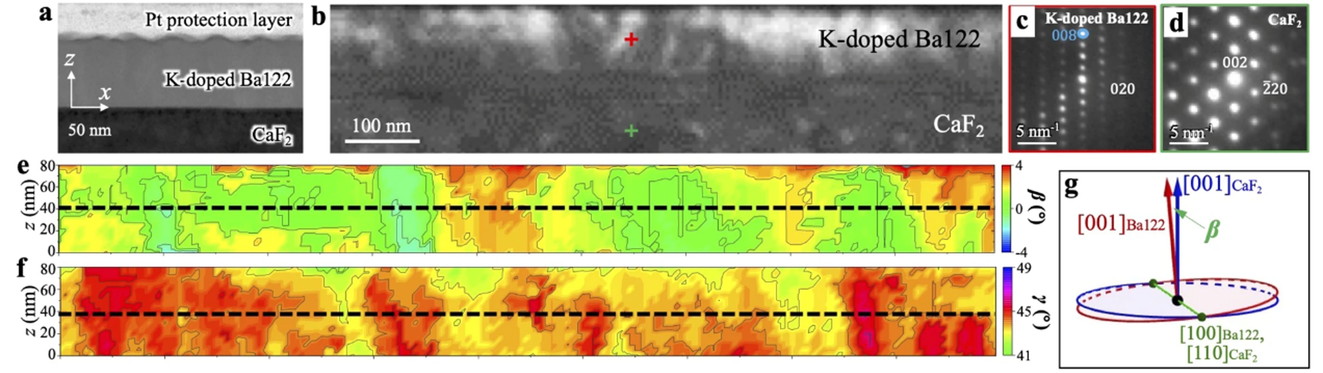
Nanoscale mapping of crystal orientation in an iron-based superconducting thin film. This enables quantitative analysis of the distribution of c-axis orientation, which strongly affects superconducting properties.
Related work: NPG Asia Materials (2021), ISIJ International (2016), etc.
Analysis of Short-Range Ordering by Atomic-Resolution STEM
Order–disorder transformations are diffusion-controlled phase transformations in which atoms or vacancies in a multicomponent crystalline solid change their arrangement on crystal lattice sites from ordered to random, or vice versa, depending on temperature and composition. Together with phase separation, this was once a central topic in TEM-based materials research. In binary A–B alloys, for example, if the position of either A or B atoms can be identified, the positions of the other atoms can also be inferred; therefore, atomic-level structural and microstructural analysis was possible even when direct atomic-resolution TEM observations were still difficult.
Although studies of order–disorder transformations may appear to be mature, changes in material properties that suggest metastable ordered phases or very fine short-range ordered regions, here referred to as nanoclusters, are still frequently discussed in materials development, for example in high-entropy alloys, aluminum alloys, and steels. Our laboratory explores methods for visualizing and analyzing nanoclusters that have not previously been identified, and seeks to understand elementary processes of deformation and the strength of metallic materials by interpreting the behavior of dislocations interacting with these clusters. We have continued collaborative studies on nanocluster analysis with research groups in India since 2010 and Norway since 2022.
For more details on our nanocluster analysis topics, please see here.
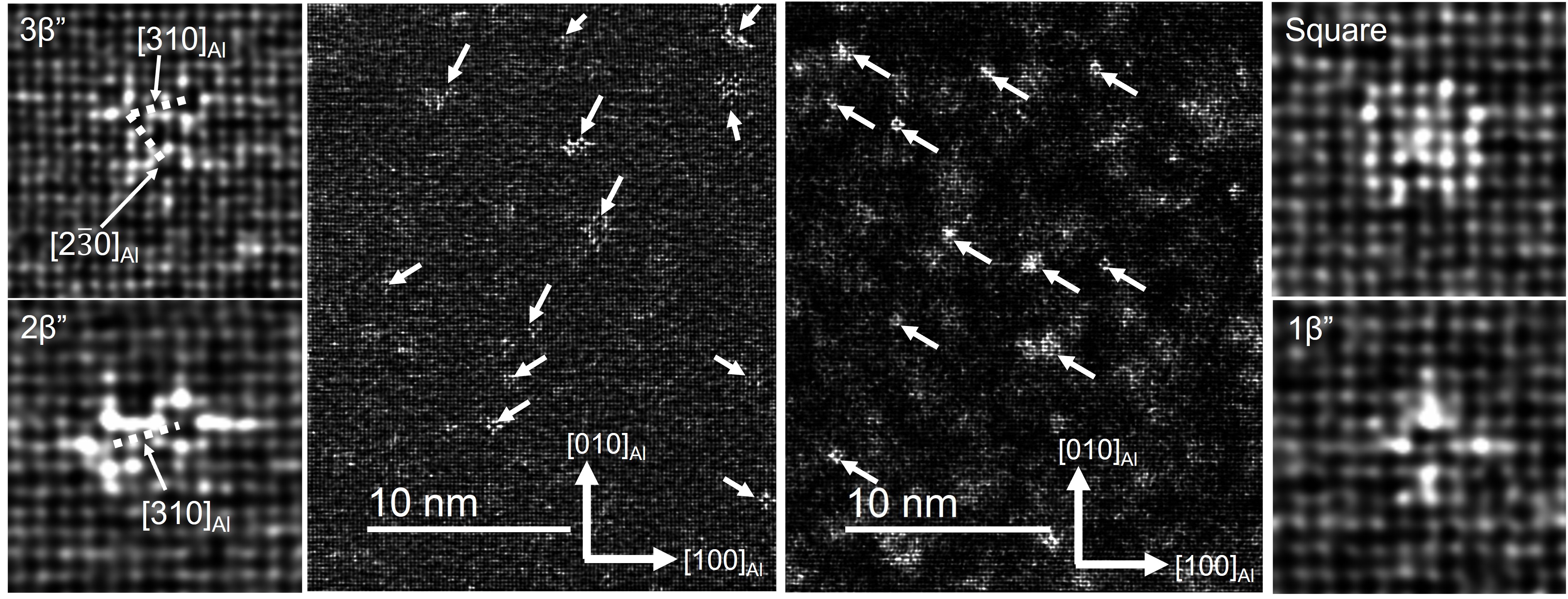
Atomic-scale imaging and analysis of nanoclusters in an aluminum alloy.
Related work: Materials Science and Engineering A (2025), etc.; collaborative research with NTNU and SINTEF since 2022.
Nanostructural Analysis of Advanced Materials
Nanostructures observed by electron microscopy are diverse and rich in information. Even when a characteristic nanostructural feature is found, it is often difficult to conclude that it is the most important factor controlling the material property of interest. Electron microscopists must therefore understand not only microscopy itself but also the materials being studied, decide which nanostructural features should be examined, and select or develop suitable observation and analysis methods. Our laboratory participates in research projects at universities, companies, and research institutes working on advanced materials, conducts practical nanostructural analysis, and develops new methods when necessary.
For more details on this topic, please see here.
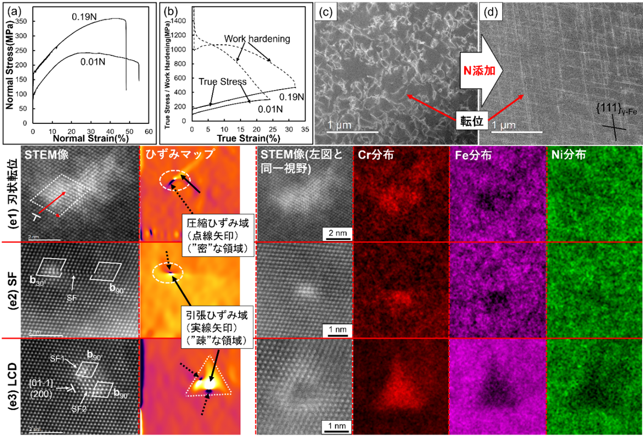
(a,b) Stress–strain curves and work-hardening curves obtained from steels. (c,d) STEM images of dislocation structures. Nitrogen addition induces planar dislocation arrays and significantly increases the work-hardening rate. (e1–e3) Atomic-resolution STEM image of the defect core structure forming the planar dislocation array, together with the corresponding strain map and elemental map obtained from the same field of view. The results suggest that Cr segregates into the tensile-strain region around the defect core due to nitrogen addition, indicating the formation of N–Cr clusters near the defect core.
Related work: Scientific Reports (2024), etc.